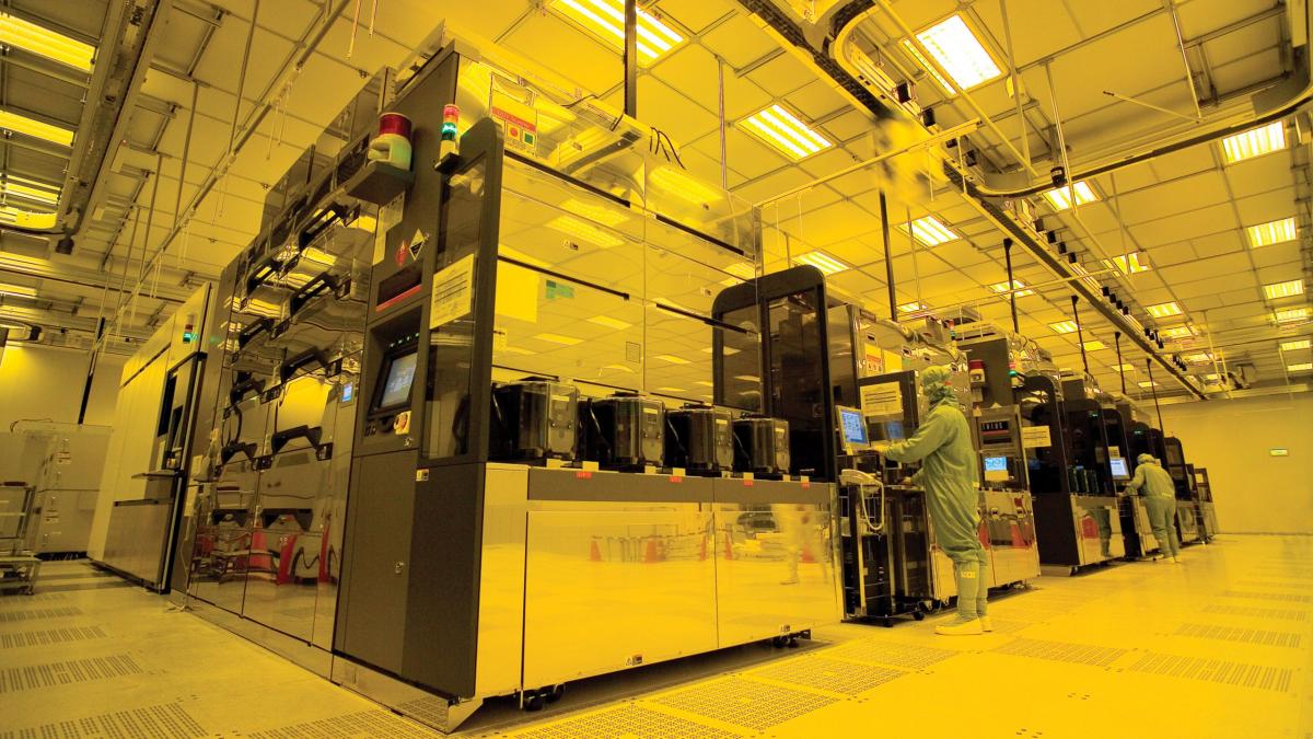
“The video shows the recently opened Fab 21 plant in the USA.”, — write: www.unian.ua
The video shows the recently opened Fab 21 plant in the USA.
 TSMC showed how they make processors / Photo – TSMCThe company TSMC published a video taken on the territory of the Fab 21 factory near Phoenix, Arizona. The footage shows a shop with hundreds of machines used to produce chips for companies such as NVIDIA, AMD and Apple.
Fab 21 is the first TSMC plant in the USA, which has already been launched into mass production using the N4 and N5 (4 and 5 nm) technological processes.
First, thin layers of materials are applied to silicon wafers – this is the basis of the future chip. Then lithography begins – a process in which a circuit diagram is “projected” onto a plate with the help of light.
After that, ASML Twinscan NXE lithography units using extreme ultraviolet (EUV) lithography come into play. It makes it possible to form miniature circuit elements with an accuracy of several nanometers, which is especially important for top chips such as the NVIDIA Blackwell B300 graphics processors used in RTX 50 graphics cards.
The video shows the “silver highway” – the automated plate delivery system (AMHS). FOUP capsules with 300 mm silicon blanks are moved along this suspension path. Each of them goes through hundreds of stages, from etching, where lasers “bite out” the desired patterns, to deposition, when new conductive or insulating layers are applied to the surface. This method of transportation maintains the stability of the process and protects the wafers from dust, because one particle can spoil the future chip.
EUV-lithography uses laser radiation with a wavelength of 13.5 nm, created by a plasma from tin droplets. After that, the plates go through a doping stage, where atoms of other elements are introduced into the crystal lattice to set the desired conductivity properties.
At the final stages, the plates are cut, tested and sent to packaging, where each crystal is placed in a case, supplied with contacts and prepared for integration into the device.
Fab 21 currently produces chips on the N4 and N5 process, but TSMC is already building the second phase of the plant, which will produce crystals at the more advanced N3 and N2 standards. The company’s general director, C. C. Wei, said that the acceleration of the transition to 2-nm and more advanced technologies is connected with the growing demand for AI chips.
We previously reported that the head of NVIDIA presented the company’s graphics chips made in the USA. The chips were just made at the TSMC Arizona plant.
You may also be interested in news:
- NVIDIA is giving away two RTX 5080s autographed by the company’s CEO
- The head of NVIDIA presented Elon Musk with the world’s smallest supercomputer
- The blogger was able to play Battlefield 6 on the screen of a water-cooled cooler
