“

Vlad Cherevko I have been interested in various types of electronics and technologies since the early 2000s. I like to play computer games and understand the operation of various gadgets. I regularly follow the news of the technology world and write materials about it myself.
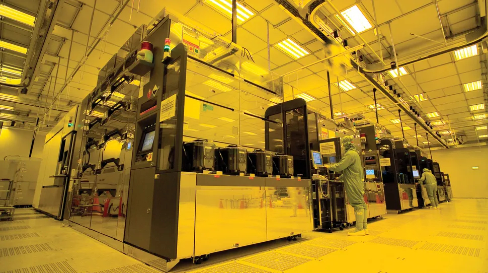
The video shows hundreds of high-tech tools for making chips, which are in a specially cleaned room with characteristic yellow lighting. It filters out short waves of light so as not to damage photoresists during chip manufacturing.
The video begins with a demonstration of the so-called “Silver Highway” — an automated material handling system (AMHS). It consists of suspended rails that move special front-opening containers (FOUPs) containing 300 mm silicon wafers. Hundreds of such containers move around the shop at the same time, which ensures accurate logistics and adherence to production cycles in a mass production environment.
 FOUP containers (frame from the video)
The central place in the video is occupied by extreme ultraviolet lithography (EUV) installations produced by the Dutch company ASML. They form the most complex elements of microcircuits, in particular for the Nvidia Blackwell B300 AI processors. The video shows the process of creating patterns on plates using radiation with a wavelength of 13.5 nm, which is generated by laser-induced plasma from tin droplets. It looks like purple flashes on camera.
EUV technology allows you to achieve a resolution of about 13 nm in half-step size per exposure cycle. At the same time, it has several disadvantages: the need for ultra-precise layering with an error of 1.1 nm, the influence of stochastic effects, and the use of mirrors instead of traditional optics, since conventional materials absorb EUV radiation. The video doesn’t show special items like custom pellicle films or wafer platforms, but TSMC is known to be applying its own modifications to these components.
Currently, the Fab 21 complex (stage 1) produces products for Apple, AMD and Nvidia. In parallel, the construction of the second stage, which will be able to produce chips according to the N3 and N2 standards, is underway.
TSMC CEO C.C. Wei also confirmed that the company is accelerating the adoption of new technologies in the US due to high demand for artificial intelligence solutions. Also, according to him, negotiations are underway to purchase an additional plot of land for the creation of a full-fledged gigafactory with a capacity of more than 100,000 plates per month.
”, — write: www.pravda.com.ua
Vlad Cherevko I have been interested in various types of electronics and technologies since the early 2000s. I like to play computer games and understand the operation of various gadgets. I regularly follow the news of the technology world and write materials about it myself.
The video shows hundreds of high-tech tools for making chips, which are in a specially cleaned room with characteristic yellow lighting. It filters out short waves of light so as not to damage photoresists during chip manufacturing.
The video begins with a demonstration of the so-called “Silver Highway” — an automated material handling system (AMHS). It consists of suspended rails that move special front-opening containers (FOUPs) containing 300 mm silicon wafers. Hundreds of such containers move around the shop at the same time, which ensures accurate logistics and adherence to production cycles in a mass production environment.
FOUP containers (frame from the video)The central place in the video is occupied by extreme ultraviolet lithography (EUV) installations produced by the Dutch company ASML. They form the most complex elements of microcircuits, in particular for the Nvidia Blackwell B300 AI processors. The video shows the process of creating patterns on plates using radiation with a wavelength of 13.5 nm, which is generated by laser-induced plasma from tin droplets. It looks like purple flashes on camera.
EUV technology allows you to achieve a resolution of about 13 nm in half-step size per exposure cycle. At the same time, it has several disadvantages: the need for ultra-precise layering with an error of 1.1 nm, the influence of stochastic effects, and the use of mirrors instead of traditional optics, since conventional materials absorb EUV radiation. The video doesn’t show special items like custom pellicle films or wafer platforms, but TSMC is known to be applying its own modifications to these components.
Currently, the Fab 21 complex (stage 1) produces products for Apple, AMD and Nvidia. In parallel, the construction of the second stage, which will be able to produce chips according to the N3 and N2 standards, is underway.
TSMC CEO C.C. Wei also confirmed that the company is accelerating the adoption of new technologies in the US due to high demand for artificial intelligence solutions. Also, according to him, negotiations are underway to purchase an additional plot of land for the creation of a full-fledged gigafactory with a capacity of more than 100,000 plates per month.